
Our product portfolio covers a wide range of LED PCB models, from office to automotive lighting. Every application has its particular demands for laminates, solder mask colours, and tolerance expectations; thus, we offer many options for
| Feature | Odak PCB's technical specifications |
|---|---|
| Number of layers | 1-2 layers |
| Materials | CEM 1, FR4, CEM 3, IMS, |
| Copper thicknesses | 35 μm - 105 μm |
| Pcb thickness | 0.4 mm to 2.4 mm |
| Minimum line width | 200 μm |
| Minimum copper to copper | 200 μm |
| Maximum panel size | 500 mm x 700 mm |
| Surface finish | Lead-Free HASL, OSP, ENIG |
| Minimum hole size | 0.5 mm |
| Solder mask colours | Warm white, cold white, green, black |
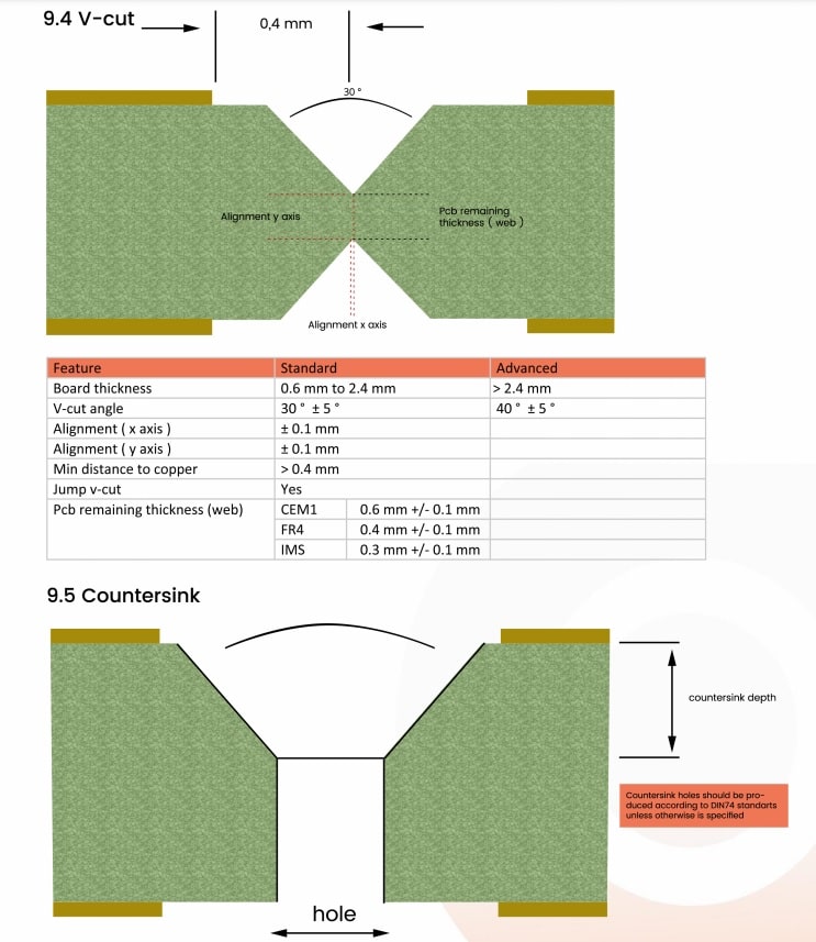
When starting a new printed circuit board design, you may spend most of your time focusing on the circuit design and component selection. However, the design might translate poorly from the digital domain to physical reality without a guideline provided by your PCB manufacturer. We have prepared a guideline for you to make the right decisions at the design stage from the very beginning.
Read More
