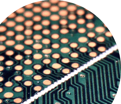

Double-sided PCBs are the most common PCB types and used in almost every industry. Improvements in PCB production capabilities and cost expectations still keep double-sided PCBs as a good option for most mid-complex designs.
| Feature | Odak PCB's technical specifications |
|---|---|
| Number of layers | 2 layer |
| Materials | FR4, CEM 3, IMS |
| Copper thicknesses | 35 μm - 105 μm |
| Pcb thickness | 0.4 mm to 2.4 mm |
| Minimum line width | 150 μm |
| Minimum copper to copper | 150 μm |
| Maximum panel size | 500 mm x 600 mm |
| Surface finish | Lead-Free HASL, OSP, ENIG, ENEPIG, Immertion silver, Immertion gold, Hard gold |
| Minimum hole size | 0.2 mm |
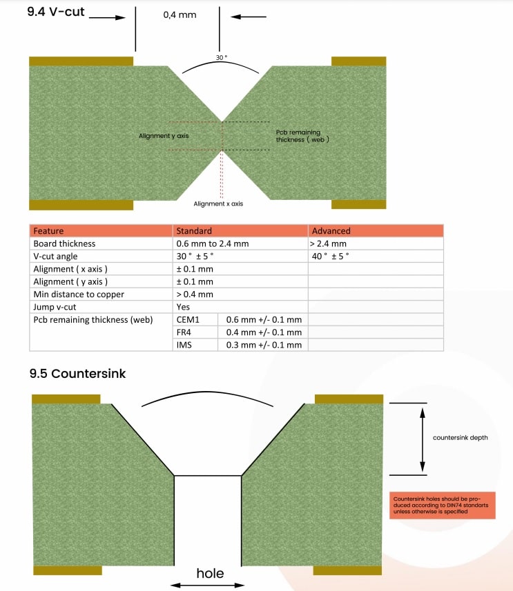
When starting a new printed circuit board design, you may spend most of your time focusing on the circuit design and component selection. However, the design might translate poorly from the digital domain to physical reality without a guideline provided by your PCB manufacturer. We have prepared a guideline for you to make the right decisions at the design stage from the very beginning.
Read More
