CAM engineers analyse Gerber files and PCB specifications provided by you and enter all product specifications into the ERP system, which are later used by both commercial and technical departments.
Customer representatives determine the quote according to technical specifications and your requested delivery date. Production begins following the order confirmation.
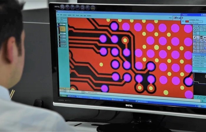
At this stage, Gerber files are processed according to PCB production parameters and efficiency. CNC, LDI, and AOI test files are generated and laser production films are plotted. Technical questions are raised here in case there is any conflict.
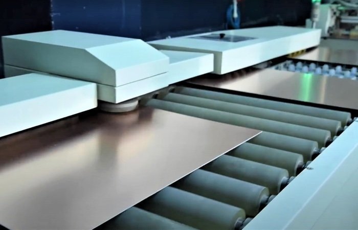
CCL (Copper Clad Laminate) is cut down into the production panel size defined on the work order form, and the edges of the panel will be bewelled for smooth handling.
Inner layers are chosen according to stack-up information provided and the layout is created on an inner layer. This process is repeated based on the stack-up structure.

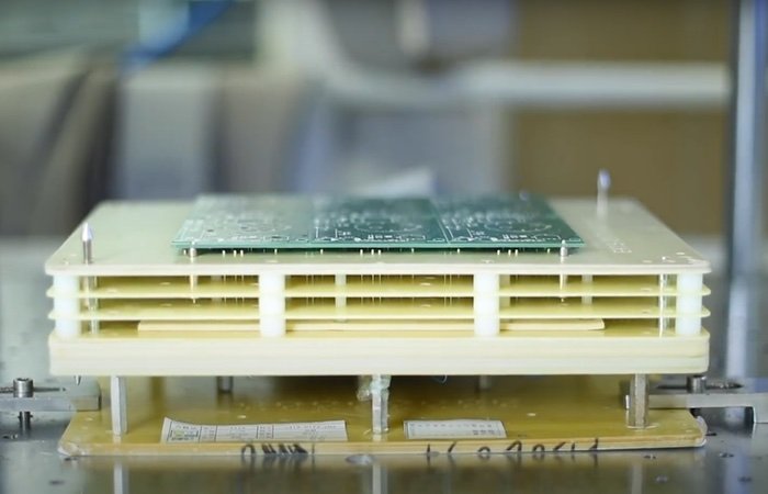
Based on the stack-up information, inner layers, prepregs, and copper foils are bonded in a multilayer hot press with suitable pressing parameters for the chosen material.

Production panels are drilled at high speed drilling machines with laser drill diameter check units. The boards are cleaned from remaining burrs and dust before the next stage.
The holes are plated with graphite, following the ultrasonic conditioning and chemical activation processes.

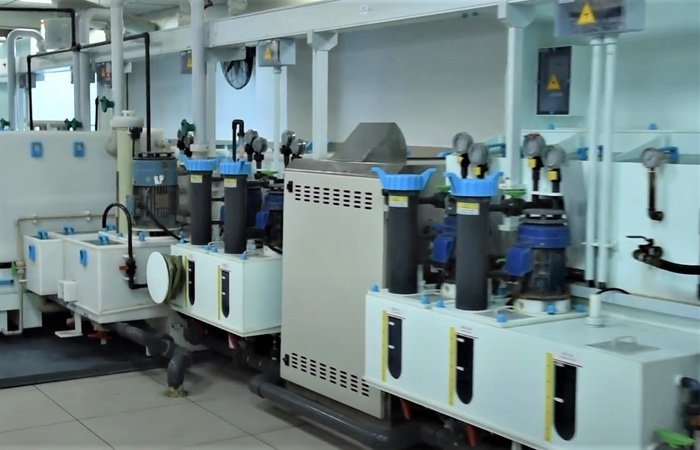
Activated holes and the surface of the PCB are electroplated with 25 μm copper to provide the connection between layers.
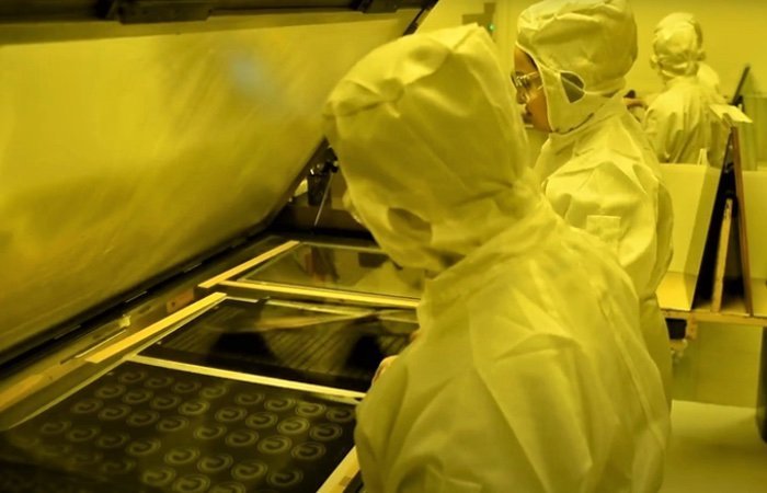
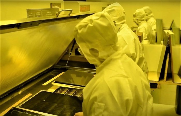
After chemical cleaning, the boards are covered with photosensitive etch resist dry films in dust-free rooms and the image is transferred by the acid-etching method.

At this stage, soldermask will be applied in dustfree rooms by leaving solderable areas open. Soldermask will be applied by 3 different curing methods as Photoimagable, Thermal and UV methods.
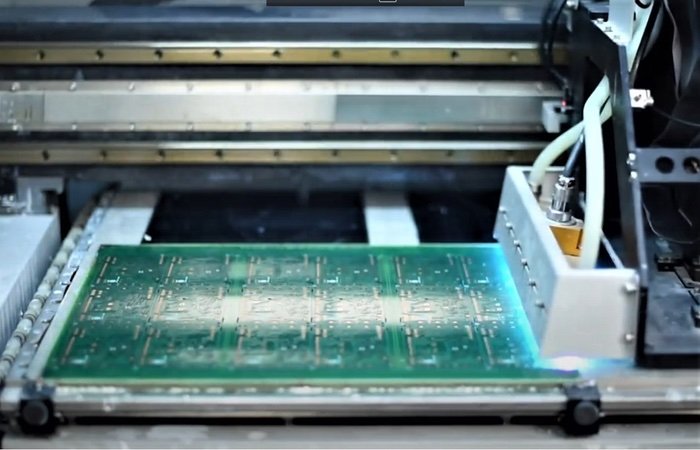
Component legend is printed either by the screen printing method or with inkjet printers.

Surface finishing types such as LF HASL, OSP, and ENIG are applied to provide easy solderability and protect solderable areas from oxidation.
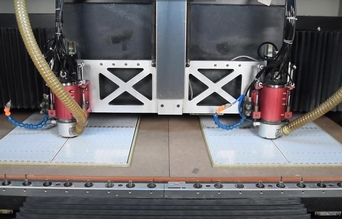
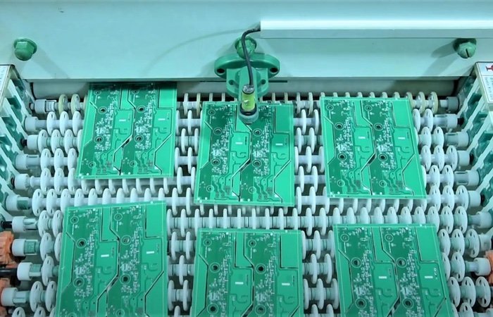
The pcb production panel will be re-sized to customer panel and customer panel will be prepared for depanelization by either routing (milling), v-cut scoring or pressing processes.
Residues that remained from the production are cleaned with high-pressure DI water in ultrasonic cleaning machines.
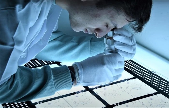
All boards that are produced must go through either fixture or flying probe testings.

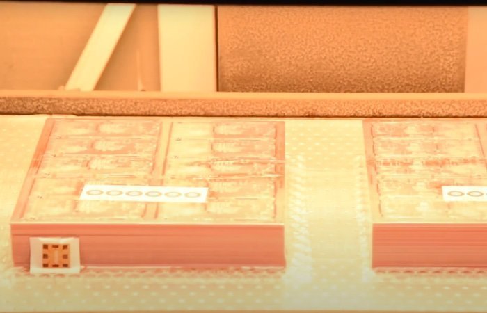
The boards are vacuum-packed with humidity indicators and silica gel to achieve the maximum shelf life. Unique labels are available upon request.